embedded systems
An Embedded system is an electronic / electromechanical system designed to perform a specific function and is a combination of both Hardware and Software. It is unique and the hardware and firmware are highly specialized to the application domain.
It’s a micro-controller or microprocessor-based system which is designed to perform a specific task. For example, a fire alarm is an embedded system; it will sense only smoke.
- Sensors: a sensor is a transducer device that converts energy from one form to another for any measurement or control purpose. Ex: Temperature Sensor, Pressure sensor.
- Actuators: An actuator is a form of transducer device (mechanical or electrical) which converts signals to corresponding physical motion. It is an output device. Ex: Electric motors, Stepper motors, LED (Light Emitting Diode).
Purpose of Embedded Systems
- Data Collection/ Storage/Representation
- Data Communication
- Data processing, Monitoring
- Control Application specific user interface.
Applications of Embedded Systems
- Consumer electronics - Televisions and digital cameras, computer printers, video game consoles and home entertainment systems like PS4
- Household appliances – Refrigerators, washing machines, microwave ovens, air conditioners
- Home automation - switching off electrical appliances like air-conditioners or refrigerators, security alarms.
- Banking and retail - Automated teller Machine (ATM)
- Measurement and Instrumentation - Digital CRO, Digital Multi meter, Logic Analyzer
- Health care - Scanners like those for MRI, CT, ECG machines devices to monitor blood pressure and heartbeat
- Automotive industry. - Airbags, anti-lock braking system, cruise control, rain-sensing wipers, emission control, traction control, automatic parking
Characteristics of an Embedded Systems
- A system which is a combination of special purpose hardware and embedded OS for executing a specific set of applications.
- May or may not contain an operating system for functioning.
- The firmware (software permanently installed in the device) of an ES is pre-programmed and it is non-alterable by the end user.
- Application-specific requirements are the key deciding factors.
- Highly tailored to take advantage of the power-saving modes supported by the hardware and the OS.
- Execution behavior is deterministic for certain types of ES like “Hard Real-Time Systems” (strict deadline).
- The response time requirement is critical for some critical systems.
- Embedded systems are created to perform the task within a certain time frame. It must, therefore, perform fast enough.
Based on Generation
- First Generation - Built around 8-bit microprocessor & micro-controller, Simple in hardware circuit & firmware developed. Ex: Digital telephone keypads
- Second Generation - Built around 16-bit μp & 8-bit μc, They are more complex & powerful than 1G μp & μc, Ex: SCADA systems Supervisory Control & Data Acquisition System
- Third Generation - Built around 32-bit μp & 16-bit μc, Concepts like Digital Signal Processors(DSPs), Application Specific Integrated Circuits(ASICs) evolved. Ex: Robotics, Media.
- Fourth Generation - Built around 64-bit μp & 32-bit μc, The concept of System on Chips (SoC), Multicore Processors evolved, Highly complex & very powerful. Ex: Smart Phones
Based on Complexity and Performance
- Small Scale Embedded Systems - Simple in application need, Performance not time-critical, Built around low-performance & low-cost 8 or 16 bit μc, Ex: Electronic toy
- Medium Scale Embedded Systems - uses a single 16-bit or 32-bit μc or multiple microcontrollers linked together. These systems have a lot of hardware as well as software complexities, hence are not preferred by many Ex: Industrial machines.
- Large Scale Embedded Systems - Built around 32 or 64 bit RISC μp/μc or PLDs or Multicore Processors, functions on multiple algorithms that result in complexities in both hardware and software. They often need a processor that is configurable and logic array that can be programmed. Response is time-critical. Ex: Mission-critical applications
Based on Deterministic Behaviour
- Deterministic/Non-Deterministic Real-time ES: Hard/Soft Real-time implies deterministic timing behavior –OS services consume only known & expected amount of time regardless of the number of services. RTOS decides which application should run in which order & how much time needs to be allocated for each application. Time Management is the basic function of RTOS. Examples: Digital camera, Thumb Impression Reader & ATM
Core of the Embedded Systems
- Embedded Systems are built around a central Core
- General Purpose and Domain Specific Processors
- Microprocessors
- Microcontrollers
- Digital Signal processors
- Application Specific Integrated Circuits (ASIC’s)
- Programmable Logic Devices (PLD’s)
- Commercial Off the Shelf Components (COTS)
microprocessor vs microcontroller
| Criteria | Microprocessor | Microcontroller |
|---|---|---|
| Description | A silicon chip representing CPU, performing ALU operations according to pre-defined set of instructions. | A highly integrated chip that contains Scratch pad RAM, special and general purpose register arrays, on-chip ROM/FLASH memory for program storage, timer and interrupt controller units and dedicated I/O ports |
| Dependency | It is a dependent unit. | It is an independent unit. |
| Design and Operation | General purpose design and operation. | Application-oriented or domain-specific. |
| Built-in I/O Ports | Doesn’t contain a built-in I/O port. | Contains multiple built-in I/O ports. |
| Target Market | Targeted for high-end market where performance is important. | Targeted for Embedded market. |
| Power Saving Options | Limited power saving options. | Includes a lot of power-saving features. |
Digital Signal Processor
- Powerful special purpose 8/16/32 bit microprocessor designed specifically to meet the computational demands and power constraints of different applications.
- 2 to 3 times faster than GPP in signal processing applications.
- It implements algorithms in hardware which speeds up the execution.
- A typical DSP incorporates the following units:
- Program Memory: storing program required by DSP.
- Data Memory: Storing temporary variables and data/signal to be processed.
- Computational Engine: Performs the signal processing in accordance with the stored program memory.
- I/O unit: Acts as an interface between the outside world and DSP (capturing signals and delivering processed signals).
- Examples: Audio-video signal processing, telecommunication and multimedia applications, real-time calculations like FFT, DFT, SOP, etc.
General Purpose Processor Vs Application Specific Instruction Set Processor
| Criteria | General Purpose Processor (GPP) | Application Specific Instruction Set Processor (ASIP) |
|---|---|---|
| Designed for | Designed for general computational tasks. Ex: laptop, Desktop | The processor contains architecture and instruction set optimized to specific domain/application requirements. Ex: SoC, DSP’s used in automotive, telecom, media applications, etc |
| Components | It contains ALU and Control Unit. | It incorporates a processor and on-chip peripherals demanded by the application requirement, program, and data memory. |
| Production and Cost | High volume of production/low cost per unit. | - |
| Role in Architectural Spectrum | - | It fills the architectural spectrum between GPP and ASIC’s. |
Application Specific Integrated Circuits (ASICs)
- It is a microchip designed to perform a specific or unique application.
- Used as a replacement for conventional general-purpose logic chips.
- It integrates several functions into a single chip and consumes very small area in the total system.
- It can be pre-fabricated for a special application or it can be custom fabricated by using the components from a re-usable building block library of components.
- Non-Recurring Engineering Charge (NRE): It is a non-refundable initial investment for the fabrication of ASICs and it is a one-time investment.
- Application Specific Standard Product (ASSP): If the Non-Recurring Engineering Charges are borne by a third party and the Application Specific Integrated Circuit (ASIC) is made openly available in the market, the ASIC is referred to as ASSP.
- Example: ADE7760 Energy Meter ASIC developed by Analog Devices for Energy Metering applications.
Programmable Logic Devices (PLDs)
PLDs can be reconfigured to perform any number of functions at any time.
Features of PLDs
- It has a wide range of logic capacity, features, speed, and voltage characteristics.
- Designers use inexpensive software tools to quickly develop, simulate, and test their designs.
- There are no Non-Recurring Engineering (NRE) costs, and the final design is completed quickly.
- PLDs are based on rewritable memory technology.
Two major types of PLDs are
- CPLDs: offer a smaller amount of logic, up to about 10,000 gates, and offer very predictable timing characteristics suitable for critical control applications.
- Example: Xilinx Coolrunner
- FPGAs: offer the highest amount of logic density, the most features, and the highest performance.
- Example: Xilinx VirtexTM.
Commercial Off-the-Shelf Components (COTS)
Provides easy integration and interoperability with existing system components. It can be developed around GPP, Domain-specific Processor, ASIC, or PLDs.
| Advantages | Disadvantages |
|---|---|
| Readily available in the market, cheap, and developers can cut down their development time to a great extent. | Due to rapid changes in technology, if the COTS component is withdrawn by the manufacturer or production is discontinued, it will adversely affect a commercial manufacturer of ES which makes use of the specific COTS product |
Memory
Memory is required for holding data temporarily during certain operations.
- On-chip memory: built-in memory.
- Off-chip memory: external memory connected with the controller/processor for storing controller algorithm.
- Program Storage Memory: Also called code storage memory of an ES, it stores the program instructions. It retains its contents even after the power to it is turned off (non-volatile storage memory).
Program Storage Memory (ROM)
Depends on fabrication, erasing, and programming technique, ROM is divided as follows:
A) Masked ROM (MROM)
- One-time Programmable device
- Uses hardwired technology to store the data
- Low cost for high volume of production
- Good candidate for storing the embedded firmware for low-cost embedded devices
- Limitation is its inability to modify the device firmware against firmware upgrades.
B) Programmable Read Only Memory (PROM / OTP)
- The end user is responsible for programming this memory
- This memory consists of polysilicon or nichrome wires functionally viewed as fuses
- Fuses which are not blown/burned represent logic “1”, whereas fuses which are blown/burned represent logic “0”
- OTP is used in commercial production of ES
C) Erasable Programmable Read Only Memory (EPROM)
- EPROM gives flexibility to re-program the same chip
- Stores bit information by charging the floating gate of an FET to a high voltage
- Contains a quartz crystal window, which is exposed to UV rays for 20 to 30 minutes to erase the entire memory
- Limitation is erasing the memory using UV rays is a tedious and time-consuming process.
D) Electrically Erasable Programmable Read Only Memory (EEPROM)
- Information contained in this memory can be erased and re-programmed in-circuit using electrical signals at register/byte level
- Provides greater flexibility for system design
- Limitation is its capacity (only a few kilobytes).
E) FLASH
- Latest ROM technology which combines the re-programmability of EEPROM and high capacity of standard ROMs
- Organized as sectors/pages
- Stores information in an array of floating gates of an MOSFET
- Each sector is erased before re-programming, done at sector/page level without affecting sector/page
- Typical erasable capacity is 1000 cycles
- Example: W27C512 from WINDBOND (64 KB FLASH memory)
F) NVRAM (Non-volatile RAM / non-volatile storage memory)
- RAM with battery backup
- Lifespan is around 10 years
- Example: DS1644 from Maxim/Dallas (32 KB NVRAM)
Read-Write Memory / Random Access
RAM: is working memory of a controller/processor where it can read from it and write to it.
Volatile in nature (requires power to maintain the stored information)
A) Static RAM (SRAM)
- It is the fastest form of RAM available (Resistive networking and Switching capabilities).
- Made up of flip-flops and stores data in the form of voltage.
- Realized using six transistors (MOSFET) out of which four are for building the latch part of the memory cell and two for controlling the access.
- Major limitation: low capacity and high cost
B) Dynamic RAM (DRAM)
- Stores the data in the form of charge
- Advantage: high density and low cost
- Disadvantage: Since it is stored as charge, it will get leaked off with time, so refreshing is needed
- Special circuits called DRAM controllers are used for refreshing the operation
Difference between SRAM and DRAM
-
SRAM
- Made up of 6 CMOS Transistors (MOSFET)
- Doesn’t require refreshing
- Low capacity
- Fast in operation. Typical access time is 10ns
-
DRAM
- Made up of a MOSFET and a capacitor
- Requires refreshing
- High Capacity
- Less expensive
- Slow in operation. Typical access time is 60ns
- Write Operation is faster than read operation
C) NVRAM (Non-volatile RAM)
- RAM with battery backup.
- Contains static RAM based memory
- Lifespan is around 10 years
- Example: DS1744 from Maxim/Dallas (32 KB NVRAM)
D) Memory according to the Type of Interface
- Parallel Interface: Parallel data lines for an 8-bit processor/controller will be connected to the memory (memory size is in terms of kilobytes)
- Serial Interface: I2C: 2-line serial interface (used for data storage memory like EEPROM, memory size is in terms of kilobits)
- Example: Atmel Corporations AT24C512 (512 K bits/ 2-wire interface)
- Serial Peripheral Interface (SPI): 2+n line interface where n stands for the total number of SPI bus devices in the system
- Single wire interconnection.
I/O Subsystem
The I/O subsystem of the embedded system facilitates the interaction of the embedded system with the external world.
- Light Emitting Diode (LED)
- 7 Segment LED display: Seven segment displays are the output display device that provides a way to display information in the form of image or text or decimal numbers.
- Optocoupler - transfers electrical signals between two isolated circuits by using light. An LED that emits infrared light and a photosensitive device that detects light from the LED.
- Stepper Motor - DC motors that move in discrete steps. Electromagnetic device that converts digital pulses into mechanical shaft rotation.
- Relay - switches that open and close circuits electro-mechanically or electronically. Either make or break a circuit.
- Piezo Buzzer - electronic device that’s used to produce a tone, alarm, or sound.
- Push Button Switch - two-position devices actuated with a button that is pressed and released.
- Keyboard - mechanisms under the key-caps on a mechanical keyboard that enable you to type faster and more precisely.
- Programmable Peripheral Interface (PPI) - general-purpose programmable I/O device designed to interface the CPU with its outside world such as ADC, DAC, keyboard, etc.
Communication Interface
- Device/ Board level communication Interface (Onboard Communication Interface)
- The communication channel which interconnects the various components within an embedded product.
- Example: Serial Interface like I2C, SPI, UART (Universal Asynchronous Receiver/Transmitter), 1-Wire & parallel bus interface
- Product level Communication Interface (External Communication Interface)
- Responsible for data transfer between the embedded system and other devices or modules.
- It can be wired media, wireless media, serial or parallel interface.
- Example: IR (Infrared), Bluetooth, Wi-Fi (Wireless Fidelity), RS232c (Recommended Standard 232), USB (Universal Serial Bus), Ethernet, etc.
Onboard communication Interfaces
- Inter Integrated Circuit (I2C)
- It is a synchronous bi-directional half duplex (devices can only transmit data in two directions but not at the same time) two-wire serial interface bus.
- Provides an easy way of connection between a microprocessor/micro controller system and the peripheral chips in television sets.
- It comprises two bus lines:
- Serial Clock (SCL): Responsible for generating synchronization clock pulses
- Serial Data (SDA): Responsible for transmitting the serial data across devices.
- It supports multimasters on the same bus.
- It supports three different data rates:
- Standard Mode: Data rate up to 100 Kbps
- Fast Mode: Data rate up to 400 Kbps
- High-Speed Mode: Data rate up to 3.4 Mbps
- It is a shared bus system. The devices connected to it can act as Master or Slave.
- Master: Responsible for controlling the communication by initiating/terminating data transfer, sending data, and generating synchronization clock pulses.
- Slave: Waits for the commands from the master and responds upon receiving commands.
- Both master and slave devices can act as either transmitter or receiver.
- The synchronisation clock signal is generated by the Master device, regardless of whether the master is acting as a transmitter or receiver.
External / Peripheral Communication Interfaces
- RS-232 C & RS-485
- Universal Serial Bus (USB)
- IEEE 1394 (Fire wire)
- Infrared (IrDA)
- Bluetooth
- Wi-Fi
- Zig Bee
- General Packet Radio Service (GPRS)
ARM Processor
- ARM stands for Advanced RISC Machines, where RISC stands for Reduced-instruction-set Computing.
- Founded in 1990, owned by Acorn, Apple, and VLSI.
- ARM is one of the most licensed and thus widespread processor cores in the world.
- Used especially in portable devices due to low power consumption and reasonable performance.
- Used in PDA, cell phones, multimedia players, handheld game consoles, digital TV, and cameras.
- ARM has several processors that are grouped into a number of families based on the processor core they are implemented with.
- The architecture of ARM processors has continued to evolve with every family.
- Some of the famous ARM Processor families are ARM7, ARM9, ARM10, and ARM11.
RISC Characteristics
Features of ARM7:
- 32-bit Processor
- 32-bit ALU
- 32-bit data bus
- 32-bit instructions
- 32-bit Address bus
- Von Neumann Architecture
- Three-stage pipelining
Spec: RS 232 C & RS 485
It is wired, asynchronous, serial, full duplex communication
- RS 232 interface was developed by EIA (Electronic Industries Associates) In early 1960s
- RS 232 is the extension to UART for external communications
- RS-232 logic levels use: +3 to +25 volts to signify a “Space” (Logic 0)
- -3 to -25 volts to signify a “Mark” (logic 1)
- RS 232 is used only for point to point connections
- It is susceptible to noise and hence is limited to short distances only
- RS 485 supports up to 32 transmitters and 32 receivers
ARM Processor Fundamentals
Data Flow Model
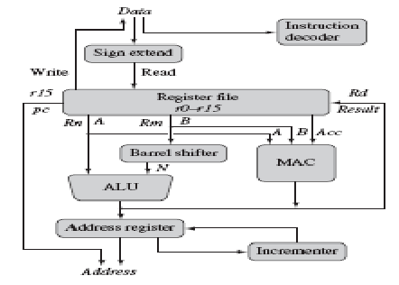
- Data enters the processor core through the data bus.
- Instruction decoder translates instructions before they are executed.
- Data items are placed in the register file-storage bank made of 32-bit registers.
- Sign extend converts signed 8-bit and 16-bit numbers to 32-bit values.
- Two source registers (Rn and Rm) and a single destination register (Rd).
- Source operands are read from the register file using internal buses A and B.
- ALU takes the register values Rn and Rm and computes the result.
- Barrel shifter computes the result for any number of shifts within a clock cycle.
- Multiply-Accumulate Circuit is used to perform both multiply and add.
- Load and store instructions use the ALU to generate an address to be held in the address register and broadcast on the Address bus.
As ARM is von Neumann architecture, the same bus is used to load instructions and data. Hence, the input data bus enters the processor core and is connected to:
-
i. Instruction decode Block
-
ii. Direct Register bank
-
iii. Sign extend hardware block (which is again connected to the register file)
-
Instruction decoder translates instructions before they are executed.
-
Data items are placed in a register file-storage bank made of 32-bit registers. Since the ARM core is a 32-bit processor, most instructions treat the registers as holding signed or unsigned 32-bit values.
-
Sign extend hardware converts signed 8-bit and 16-bit numbers to 32-bit values as they are read from memory and placed in a register.
Basic Processing Units
i. ALU (Arithmetic Logic Unit) ii. Barrel Shifter iii. MAC (Multiply and Accumulate Unit)
ALU (Arithmetic and Logical Unit)
- ALU takes values Rn and Rm and computes results.
- ALU performs add, sub, etc. (mathematical operations), OR/AND, etc. (logical operations) on the data present in data registers.
- Load and store instructions use the ALU to generate an address to be held in the address register and broadcast on the Address bus.
Barrel Shifter
A barrel shifter is a digital circuit that can shift a data word by a specified number of bits in one clock cycle.
- Operand 2 (B) can be directly loaded or shifted by a specified number of times.
- Can achieve fast multiplication or division by a power of 2.
MAC (Multiply and Accumulate Unit)
- Multiply-Accumulate Circuit is used to perform both multiplication and addition.
- The result of any operation can be written back to the register bank.
- Supports basic summation operation on data present in registers.
Address Register
- Contains the address from which data or instruction needs to be fetched. (like start address)
- This register is connected to the Incrementer unit.
Registers
- Stack Pointer: Stores the head of the stack in the current processor mode.
- Link Register: Core puts the return address when it calls a subroutine.
- Program Counter: Contains the address of the next instruction to be fetched by the processor.
- In ARM state, the registers R0 – R15 are orthogonal (instruction type & addressing mode vary independently).
- Any instruction that you can apply to R0 can equally well apply to other registers.
Current Program Status Register (CPSR)
- 32-bit register.
- Contains the present status of an internal operation.
- ARM uses CPSR to monitor and control internal operations.
- CPSR is a dedicated 32-bit register and resides in the register file.
- A generic program status register.
Processor Modes
- The processor mode determines which registers are active and the access rights to the CPSR register itself.
- Privileged mode allows full read-write access to CPSR:
- Abort
- Fast interrupt request
- Interrupt request
- Supervisor
- System
- Undefined
- Non-privileged mode:
- Read access to control field to CPSR.
- Read-write access to conditional flags.
- User.
- Privileged mode allows full read-write access to CPSR:
The ARM has seven operating modes:
- User (unprivileged mode under which most tasks run).
- FIQ (entered when a high priority (fast) interrupt is raised).
- IRQ (entered when a low priority (normal) interrupt is raised).
- Supervisor (entered on reset and when a Software Interrupt instruction is executed).
- Abort (used to handle memory access violations).
- Undefined (used to handle undefined instructions).
- System (privileged mode using the same registers as user mode).
Banked Registers
- ARM has 37 registers in total, all of which are 32-bits long.
- 1 dedicated program counter
- 1 dedicated current program status register
- 5 dedicated saved program status registers
- 30 general-purpose registers
- 20 registers are hidden from a program at different times. These registers are called banked registers.
- They are available only when the processor is in a particular mode.
State and Instruction Sets
The state of the core determines which instruction set is being executed.
- ARM State: A processor in one instruction set state cannot execute instructions from another instruction set. A processor in ARM state cannot execute Thumb instructions.
- Thumb State: Thumb mode provides greater code density, at the expense of speed.
- Jazelle State: Jazelle (direct bytecode execution) is an extension that allows some ARM processors to execute Java bytecode in hardware as a third execution state.
prev: communication