Computer Organization
NOTE
Computer organization refers to the internal structure and design of a computer system.
Types of Computers
Example
- Embedded computers: integrated into a larger device or system in order to automatically monitor and control a physical process / environment. They are used for a specific purpose rather than for general processing tasks.
- PCs: desktops, laptops, et-al
- Servers and Enterprise: large computers that are meant to be shared by a large number of users who access them from some form of personal computer over a VPN.
- Supercomputers: Grid computers with the highest performance computations needed in weather forecasting, engineering design and simulation, and scientific work. Grid computers provide a more cost-effective alternative. They combine a large number of personal computers and disk storage units in a physically distributed high-speed network, called a grid.
Functional Units
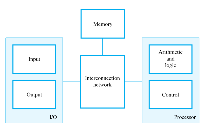
A computer consists of five functionally independent main parts: input, memory, arithmetic and logic, output, and control units.
Info
We refer to the arithmetic and logic circuits, with the main control circuits, as the processor and the input and output hardware as the I/O units.
Question
The computer is controlled by the stored program, except for possible external interruption by an operator or by I/O devices connected to it.
Input Unit
Whenever a key is pressed, the corresponding letter or digit is automatically translated into its corresponding binary code and transmitted to the processor.
Memory Unit
The function of the memory unit is to store programs and data. There are two classes of storage, called primary and secondary.
Main memory, is a fast memory that operates at electronic speeds. Programs must be stored in this memory while they are being executed.
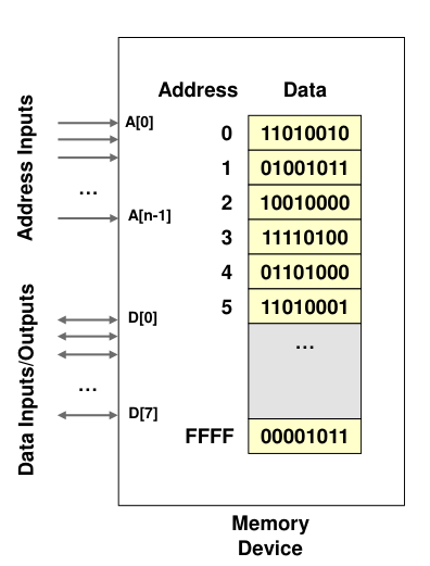
The memory consists of a large number of semiconductor storage cells, each capable of storing one bit of information. These cells are rarely read or written individually. Instead, they are handled in groups of fixed size called words. The memory is organized so that one word can be stored or retrieved in one basic operation. The number of bits in each word is referred to as the word length of the computer, typically 16, 32, or 64 bits.
To provide easy access to any word in the memory, a distinct address is associated with each word location. Addresses are consecutive numbers, starting from 0, that identify successive locations. A particular word is accessed by specifying its address and issuing a control command to the memory that starts the storage or retrieval process. Instructions and data can be written into or read from the memory under the control of the processor. The time required to access one word is called the memory access time.
Cache Memory: smaller, faster RAM unit, called a cache, is used to hold sections of a program that are currently being executed, along with any associated data. The cache is tightly coupled with the processor and is usually contained on the same integrated-circuit chip. The purpose of the cache is to facilitate high instruction execution rates.
Tip
A program is a list of instructions which performs a task. Programs are stored in the memory.
It is convenient to categorize this information as either instructions or data. Instructions, or machine instructions, are explicit commands that:
- Govern the transfer of information within a computer as well as between the computer and its I/O devices.
- Specify the arithmetic and logic operations to be performed.
At the start of program execution, the cache is empty. All program instructions and any required data are stored in the main memory. As execution proceeds, instructions are fetched into the processor chip, and a copy of each is placed in the cache. The data is fetched and copies are also placed in the cache.
If the same data locations are accessed repeatedly while copies of their contents are available in the cache, they can be fetched quickly.
Memory Operations
Both program instructions and data operands are stored in the memory. To execute an instruction, the processor control circuits must cause the word (or words) containing the instruction to be transferred from the memory to the processor.
Operands and results must also be moved between the memory and the processor. Thus, two basic operations involving the memory are needed, namely, Read and Write.
Info
The Read operation transfers a copy of the contents of a specific memory location to the processor. The memory contents remain unchanged. To start a Read operation, the processor sends the address of the desired location to the memory and requests that its contents be read. The memory reads the data stored at that address and sends them to the processor.
Info
The Write operation transfers an item of information from the processor to a specific memory location, overwriting the former contents of that location. To initiate a Write operation, the processor sends the address of the desired location to the memory, together with the data to be written into that location.
Secondary Storage (I/O)
Additional, less expensive, permanent secondary storage is used when large amounts of data and many programs have to be stored, particularly for information that is accessed infrequently. Access times for secondary storage are longer than for primary memory. A wide selection of secondary storage devices is available.
Output Unit (I/O)
Touchscreens: the dual role of such units is the reason for using the single name input/output (I/O) unit in many cases.
Memory vs I/O Access
Processor performs reads and writes to communicate with memory and I/O devices. I/O devices have memory locations that contain data that the processor can access.
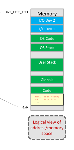 All memory locations (be it RAM or I/O) have unique addresses which are used to identify them. The assignment of memory addresses is known as the physical memory map.
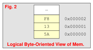
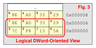
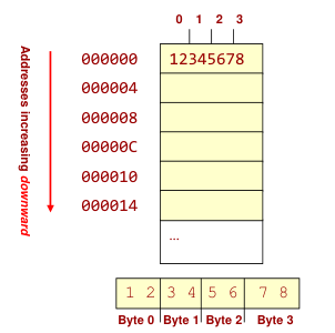
Because each byte of memory has its own address we can picture memory as one column of bytes (Fig. 2). But, 64-bit logical data bus allows us to access up to 8-bytes of data at a time. We will usually show memory arranged in rows of 4-bytes (Fig. 3) or 8-bytes, still with separate addresses for each byte.
Arithmetic and Logic Unit
Math: +-*/, comparison of numbers is initiated by bringing the required operands into the
processor, where the operation is performed by the ALU.
The sum may then be stored in the memory or retained in the processor for immediate use. When operands are brought into the processor, they are stored in high-speed storage elements called registers. Each register can store one word of data. Access times to registers are even shorter than access times to the cache unit on the processor chip.
Question
What if we didn’t have registers?
F = (X+Y) – (X*Y)requires anADDinstruction,MULtiply instruction andSUBtract instruction.
- ADD: Load X, Y from memory and store the result to memory.
- MUL: Load X, Y from memory and store the result to memory.
- SUB: Load results from ADD and MUL and store the result to memory.
Warning
(9 memory access!!)
Success
- Load X and Y into registers
- ADD: R0 + R1 and store result in R2
- MUL: R0 * R1 and store result in R3
- SUB: R2 – R3 and store result in R4
- Store R4 back to memory
- 3 total memory access
Control Unit
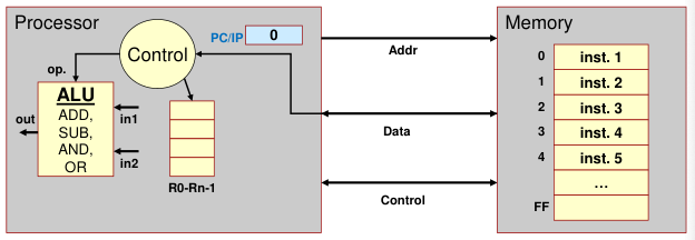
The memory, arithmetic and logic, and I/O units store and process information and perform input and output operations. The operation of these units must be coordinated in some way. This is the responsibility of the control unit. It sends control signals to other units and senses their states.
Info
- Controls the ALU
- Selects Registers to be used as source and destination locations
I/O transfers, consisting of input and output operations, are controlled by program instructions that identify the devices involved and the information to be transferred.
Control circuitry is used to decode the instruction and then generate the necessary signals to complete its execution.
Example
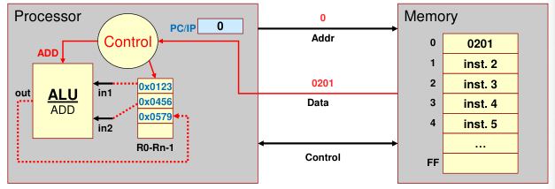
Assume
0x0201is machine code for an ADD instruction ofR2 = R0 + R1Control Logic will
- select the registers (R0 and R1)
- tell the ALU to add
- select the destination register (R2)
Control circuits are responsible for generating the timing signals that govern the transfers and determine when a given action is to take place. Data transfers between the processor and the memory are also managed by the control unit through timing signals. It is reasonable to think of a control unit as a well-defined, physically separate unit that interacts with other parts of the computer.
Program Flow
Execution of the program begins when the PC is set to point to the first instruction of the program. The contents of the PC are transferred to the memory along with a Read control signal. When the addressed word (in this case, the first instruction of the program) has been fetched from the memory it is loaded into register IR. At this point, the instruction is ready to be interpreted and executed.
Instructions such as Load, Store, and Add perform data transfer and arithmetic opera- tions. If an operand that resides in the memory is required for an instruction, it is fetched by sending its address to the memory and initiating a Read operation. When the operand has been fetched from the memory, it is transferred to a processor register.
After operands have been fetched in this way, the ALU can perform a desired arithmetic operation, such as Add, on the values in processor registers. The result is sent to a processor register. If the result is to be written into the memory with a Store instruction, it is transferred from the processor register to the memory, along with the address of the location where the result is to be stored, then a Write operation is initiated.
The contents of the PC are incremented so that the PC points to the next instruction to be executed. Thus, as soon as the execution of the current instruction is completed, the processor is ready to fetch a new instruction.
Instruction Cycle
It performs the same 3-step process over and over again
- Fetch an instruction from memory
- Decode the instruction: Is it an
ADD,SUB, etc.? - Execute the instruction: Perform the specified operation
Opcodes
A typical instruction might be:
Load R2, LOC
Info
This instruction reads the contents of a memory location whose address is represented symbolically by the label
LOCand loads them into processor registerR2. The original contents of location LOC are preserved, whereas those of register R2 are overwritten.
Execution of this instruction requires several steps. First, the instruction is fetched from
the memory into the processor. Next, the operation to be performed is determined by the
control unit. The operand at LOC is then fetched from the memory into the processor. Finally, the operand is stored in register R2. After operands have been loaded from memory into processor registers, arithmetic or logic operations can be performed on them.
For example, the instruction.
Add R4, R2, R3
After completing the desired operations, the results are in processor registers. They
can be transferred to the memory using instructions such as: Store R4, LOC
Notice how the notation is inverted: For Load and Store instructions, transfers between the memory and the processor are initiated by sending the address of the desired memory location to the memory unit and asserting the appropriate control signals.
Quote
The instruction register (IR) holds the instruction that is currently being executed. Its output is available to the control circuits, which generate the timing signals that control the various processing elements involved in executing the instruction.
The program counter (PC) is another specialized register. It contains the memory address of the next instruction to be fetched and executed. During the execution of an instruction, the contents of the PC are updated to correspond to the address of the next instruction to be executed. PC points to the next instruction that is to be fetched from the memory.
Then, there are general-purpose registers R0 through Rn−1 , often called processor registers. They serve a variety of functions, including holding operands that have been loaded from the memory for processing.
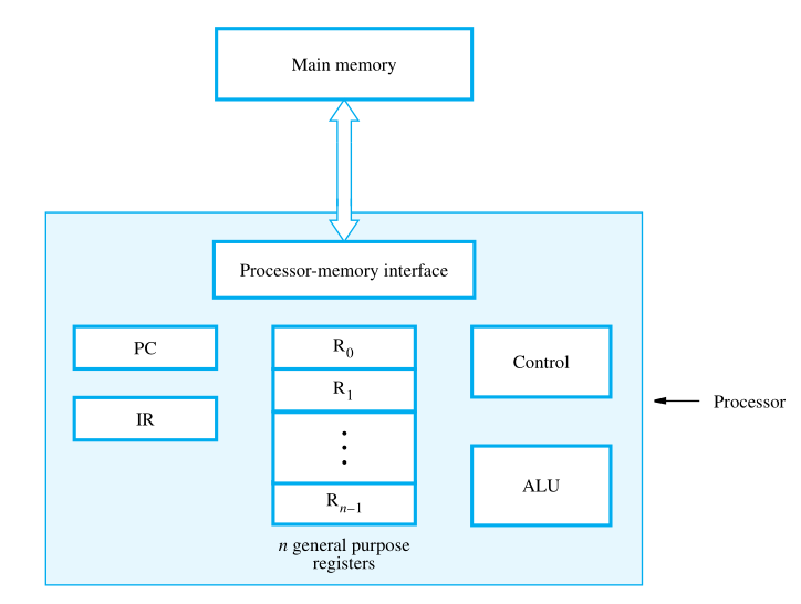
If a word is to be read from the memory, the interface sends the address of that word to the memory along with a Read control signal. The interface waits for the word to be retrieved, then transfers it to the appropriate processor register. If a word is to be written into memory, the interface transfers both the address and the word to the memory along with a Write control signal.
x86-64 Instruction Classes
Example
- Data Transfer (mov instruction)
- Moves data between processor & memory (loads and saves variables between processor and memory)
- One operand must be a processor register (can’t move data from one memory location to another)
- Specifies size via a suffix on the instruction
(movb, movw, movl, movq)- ALU Operations
- One operand must be a processor register
- Size and operation specified by instruction
(addl, orq, andb, subw)- Control / Program Flow
- Unconditional/Conditional Branch
(cmpq, jmp, je, jne, jl, jge)- Subroutine Calls (call, ret)
- Privileged / System Instructions – Instructions that can only be used by OS or other “supervisor” software (e.g. int to access certain OS capabilities, etc).
Interrupts
In order to respond immediately, execution of the current program must be suspended. To cause this, the device raises an interrupt signal, which is a request for service by the processor. The processor provides the requested service by executing a program called an interrupt-service routine.
Such diversions may alter the internal state of the processor, its state must be saved in the memory before servicing the interrupt request. Normally, the information that is saved includes the contents of the PC, the contents of the general-purpose registers, and some control information. When the interrupt-service routine is completed, the state of the processor is restored from the memory so that the interrupted program may continue.
Interrupt latency
In program-controlled I/O, when the processor continuously monitors the status of the device, it does not perform any useful tasks.
- Saving and restoring information can be done automatically by the processor
- Saving and restoring registers involves memory transfers:
- Increases the total execution time.
- Increases the delay between the time an interrupt request is received, and the start of execution of the interrupt-service routine. This delay is called interrupt latency.
- In order to reduce the interrupt latency, most processors save only the minimal amount of information:
- This minimal amount of information includes Program Counter and processor status registers.
- Any additional information that must be saved, must be saved explicitly by the program instructions at the beginning of the interrupt service routine.
Interrupt Enable & Disable
- Interrupt-requests interrupt the execution of a program, and may alter the intended sequence of events:
- Sometimes such alterations may be undesirable, and must not be allowed.
- Processors generally provide the ability to enable and disable such interruptions as desired.
- One simple way is to provide machine instructions such as Interrupt-enable and Interrupt-disable for this purpose.
Avoidance of successive interrupts
- The interrupt request signal will be active until it learns that the processor has responded to its request. It is essential to ensure that this active signal does not lead successive interrupts.
- Several mechanism are available to solve this problem:
- The interrupt be disabled/enabled in the interrupt-service routine.
- The processor automatically disable interrupts before starting the execution of the interrupt-service routine.
- The processor has a special interrupt request line through which it receives only one interrupt request regardless how long the line is activated.
Handdling single device ISR
- The device raises an IR
- The processor interrupt the program currently being executed.
- Interrupts are disabled by changing bit in PS
- The device is informed that its request has been recognized & in response, it deactivates the IR signal
- The action requested by the interrupt is performed by ISR
- Interrupts are enabled & execution of the interrupted program is resumed.
Vectored Interrupts
- To reduce the time involved in polling process, a device requesting an interrupt may identify itself directly to the processor.
- Then the processor can immediately start executing the corresponding ISR.
- A device requesting an interrupt can identify itself by sending a special code to the processor over the bus.
- The code supplied by the device may represent the starting address of the ISR for that device.
- The interrupt vector may also include a new value for the processor status register.
- When a device generates an interrupt request, the processor may not be ready to receive the interrupt_vector code immediately.
- Ex. It must first complete the execution of current instruction which may require the use of bus
- The interrupting device must wait to put data on the bus only when the processor is ready to receive it
- When the processor is ready to receive the interrupt_vector code, it activates the interrupt_acknowledgement line, INTA.
- The I/O device responds by sending the interrupt_vector code and de-activating the INTR signal.
Nesting Interupts
- This example suggests that I/O devices should be organized in a priority structure.
- An interrupt request from a high priority device should be accepted while the processor is servicing another request from a lower priority device.
- To implement this scheme, we can assign a priority level to the processor that can be changed under program control.
- The priority level of the processor is the priority of the program that is currently being executed.
- This action disables interrupt from devices at the same level of priority or lower.
- However, interrupt requests from higher priority devices will continue to be accepted.
- The processor’s priority is usually encoded in a few bits of the processor status word.
- This can be changed by privileged instructions, which are executed only while the processor is serving in the supervisor mode.
- The processor is in the supervisor mode only when executing operating system routines.
- It switches to the user mode before beginning to execute application programs.
- If a user program accidentally or intentionally, changes the priority of the processor and disrupt the system operation, will lead to a special type of interrupt called a privilege exception.
- Implementation of interrupt priority using individual interrupt-request & acknowledgement lines is as shown
Simultaneous Requests
-
Consider the problem of simultaneous arrivals of interrupt requests from two or more devices.
-
The processor must have some means of deciding which request to service first.
-
If all the devices have individual interrupt-request lines then using a priority scheme, the processor accepts the request having the highest priority.
-
If all the devices share a common interrupt-request line, some other mechanism is needed.
-
Polling the status registers of the I/O devices, in which priority is determined by the order in which the devices are polled.
-
In vectored interrupts, we must ensure that only one device is selected to read its vectored interrupt code.
-
For this a widely used scheme is to connect the devices to form a daisy chain

- the interrupt request line INTR is common to all devices
- the interrupt acknowledge line INTA is connected in a daisy chain fashion, such that the INTA signal propagates serially through the devices
- When INTR is active the processor responds by setting INTA to 1
- This signal is received by device1 , and passes it to device2 only if it does not require any service.
- If the Device 1 has pending request for interrupt, it blocks the INTA signal and proceeds to put its identifying code on the data lines
- The device closest to cpu has higher priority
- Devices are organized in groups and each group is connected at a different priority level.
- Within a group devices are inter-connected in a daisy chain
- Arrangement of priority groups as shownMachine Instructions and Programs
Exceptions
Error
Interrupts caused by interrupt-requests sent by I/O devices.
Interrupts could be used in many other situations where the execution of one program needs to be suspended and execution of another program needs to be started.
Example
- Interrupt-requests from I/O devices is one type of an exception.
- Other types of exceptions are:
- Recovery from errors
- Debugging
- Privilege exception
Example
Many sources of errors in a processor. For example:
- Error in the data stored.
- Error during the execution of an instruction.
- When such errors are detected, exception processing is initiated.
- Processor takes the same steps as in the case of I/O interrupt-request.
- It suspends the execution of the current program, and starts executing an exception-service routine.
Question
Difference between handling I/O interrupt-request and handling exceptions due to errors:
- In case of I/O interrupt-request, the processor usually completes the execution of an instruction in progress before branching to the interrupt-service routine.
- In case of exception processing however, the execution of an instruction in progress usually cannot be completed
Number Representation
We need to represent both positive and negative numbers. Three systems are used for representing such numbers:
- Sign-and-magnitude
- 1’s-complement
- 2’s-complement
In all three systems, the leftmost bit is 0 for positive numbers and 1 for negative numbers.
In the sign-and-magnitude system, negative values are represented by changing the most bit from 0→1.
In 1’s-complement representation, negative values are obtained by complementing each
bit of the corresponding positive number. Thus, the representation for -3 is obtained
by complementing each bit 0011 → 1100. Converting either way is referred to as forming the 1’s-complement of a given number.
In the 2’s-complement system, forming the 2’s-complement of an n-bit number is done by subtracting the number from 2n . Hence, the 2’s-complement of a number is obtained by adding 1 to the 1’s-complement of that number.
Addition and subtraction of n-bit using the 2’s
-
To add two numbers, add their n-bit representations, ignoring the carry-out bit from the (MSB). The sum will be the algebraically correct value in 2’s-complement representation if the actual result is in the range
−2n−1through+2n−1 − 1. -
To subtract two numbers X and Y , that is, to perform
X − Y, form the 2’s-complement of Y, then add it to X using the add rule. Again, the result will be the algebraically correct value in 2’s-complement representation if the actual result is in the range−2n−1through+2n−1 − 1.
Sign Extension
We often need to represent a value given in a certain number of bits by using a larger number of bits. For a positive number, this is achieved by adding 0s to the left. For a negative number in 2’s-complement representation, the leftmost bit, which indicates the sign of the number, is a 1. A longer number with the same value is obtained by replicating the sign bit to the left as many times as needed.
Floating Point
- a sign for the number
- some significant bits
- a signed scale factor exponent for an implied base of 2
Instruction Set Architecture
Quote
The way programs are executed in a computer from the machine instruction set viewpoint.
A complete instruction set, including operand addressing methods, is often referred to as the instruction set architecture (ISA) of a processor.
Memory Locations and Addresses
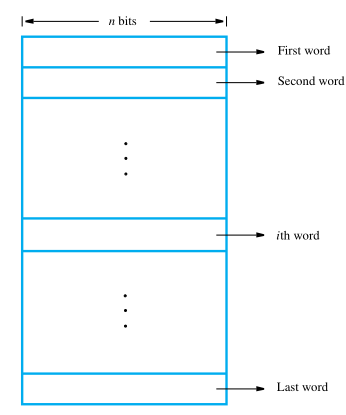
Because a single bit represents a very small amount of information, bits are never handled individually. The usual approach is to deal with them in groups of fixed size. The memory of a computer can be schematically represented as a collection of words.
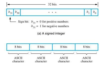
If word length of a computer is 32 bits, a single word can store a 32-bit signed number or four ASCII-encoded characters, each occupying 8 bits. Machine instructions may require one or more words for their representation.
Endian-ess
Quote
Endian-ness refers to the two alternate methods of ordering the bytes in a larger unit (word, DWORD, etc.)
Important
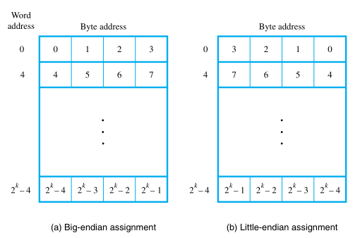
The name big-endian is used when lower byte addresses are used for the more significant bytes (the leftmost bytes) of the word.
The name little-endian is used for the opposite ordering, where the lower byte addresses are used for the less significant bytes (the rightmost bytes) of the word.
In addition to specifying the address ordering of bytes within a word, it is also necessary to specify the labeling of bits within a byte or a word. The most common convention, is the most natural ordering for the encoding of numerical data.
| Little | Big |
|---|---|
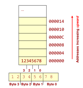
| makes sense if you view your memory as starting at the bottom-right and addresses increasing as you go up | makes sense if you view your memory as starting at the top-left and addresses increasing as you go down |
| MS byte is put at the starting address | LS byte is put at the starting address |
 |  |
Some processors (like ARM) and busses can be configured for either big / little-endian
Word Alignment
In the case of a 32-bit word length, natural word boundaries occur at addresses 0, 4, 8.. We say that the word locations have aligned addresses if they begin at a byte address that is a multiple of the number of bytes in a word.
Hence, if the word length is 16 (2 bytes), aligned words begin at byte addresses 0, 2, 4.. and for a word length of 64 (23 bytes), aligned words begin at byte addresses 0, 8, 16, ..
There is no reason you can’t have unaligned words, at an arbitrary word address.
Instructions and Instruction Sequencing
The tasks carried out by a computer program consist of a sequence of small steps, such as adding two numbers, testing for a particular condition, reading a character from the keyboard, or sending a character to be displayed on a display screen. A computer must have instructions capable of performing four types of operations:
- Data transfers between the memory and the processor registers
- Arithmetic and logic operations on data
- Program sequencing and control
- I/O transfers
To do this, we need a kind of notation!
Register Transfer Notation
Possible locations that may be involved in such transfers are memory locations, processor registers, or registers in the I/O subsystem. Most of the time, we identify such locations symbolically with convenient names. For example, names that represent the addresses of memory locations may be LOC, PLACE, A, or VAR2. Predefined names for the processor registers may be R0 or R5.
Registers in the I/O subsystem may be identified by names such as DATAIN or OUTSTATUS. This R2 ← [LOC] means: the contents of memory location LOC are transferred into processor register R2.
RTN
This type of notation is known as Register Transfer Notation (RTN). Note that the right hand side of an RTN expression always denotes a value, and the left-hand side is the name of a location where the value is to be placed, overwriting the old contents of that location.
Assembly-Language Notation
We need another type of notation to represent machine instructions and programs. For this, we use assembly language. For example, a generic instruction that causes the transfer described above, from memory location LOC to processor register R2, is specified by the statement Load R2, LOC
The contents of LOC are unchanged by the execution of this instruction, but the old contents of register R2 are overwritten.
The name Load is appropriate for this instruction, because the contents read from a memory location are loaded into a processor register.
The second example of adding two numbers contained in processor registers
R2andR3and placing their sum inR4can be specified by the assembly-language statementAdd R4, R2, R3In this case, registersR2andR3hold the source operands, whileR4is the destination.
RISC and CISC Instruction Sets
Info
There are two fundamentally different approaches in the design of instruction sets for modern computers. One popular approach is based on the premise that higher performance can be achieved if each instruction occupies exactly one word in memory, and all operands needed to execute a given arithmetic or logic operation specified by an instruction are already in processor registers.
This approach is conducive to an implementation of the processing unit in which the various operations needed to process a sequence of instructions are performed in “pipelined” fashion to overlap activity and reduce total execution time of a program. The restriction that each instruction must fit into a single word reduces the complexity and the number of different types of instructions that may be included in the instruction set of a computer.
Warning
An alternative to the RISC approach is to make use of more complex instructions which may span more than one word of memory, and which may specify more complicated operations. This approach was prevalent prior to the introduction of the RISC approach.
Tip
Two key characteristics of RISC instruction sets are:
- Each instruction fits in a single word.
- A load/store architecture is used, in which:
- Memory operands are accessed only using Load and Store instructions.
- All operands involved in an arithmetic or logic operation must either be in processor registers, or one of the operands may be given explicitly within the instruction word.
At the start of execution of a program, all instructions and data used in the program are stored in the memory of a computer. Processor registers do not contain valid operands at that time. If operands are expected to be in processor registers before they can be used by an instruction, then it is necessary to first bring these operands into the registers.
This task is done by Load instructions which copy the contents of a memory location into a processor register. Load instructions are of the form
Load processor_register, memory_location
To carry out this action, C ← [A] + [B] the contents of memory locations A
and B are fetched from the memory and transferred into the processor where their sum is computed. This result is then sent back to the memory and stored in location C.
The required action can be accomplished by a sequence of simple machine instructions. We choose to use registers R2, R3, and R4 to perform the task with four instructions:
Load R2, A
Load R3, B
Add R4, R2, R3
Store R4, C
Important
Observe that in the Store instruction the source and destination are specified in the reverse order from the Load instruction; this is a commonly used convention.
We can accomplish the desired addition by using only two registers, R2 and R3, if one of the source registers is also used as the destination for the result. In this case the addition would be performed as Add R3, R2, R3 and Store R3, C
Let us consider how this program is executed.
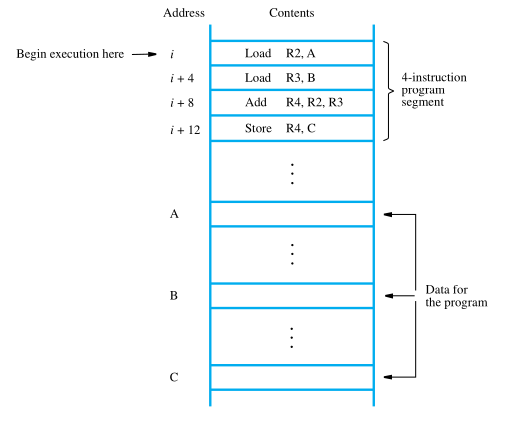
To begin executing a program, the address of its first instruction (i in our example) must be placed into the PC. Then, the processor control circuits use the information in the PC to fetch and execute instructions, one at a time, in the order of increasing addresses.
This is called straight-line sequencing. During the execution of each instruction, the PC is incremented by 4 to point to the next instruction. Thus, after the Store instruction at location i + 12 is executed, the PC contains the value i + 16, which is the address of the first instruction of the next program segment.
Executing a given instruction is a two-phase procedure. In the first phase, called instruction fetch, the instruction is fetched from the memory location whose address is in the PC. This instruction is placed in the instruction register (IR) in the processor. At the start of the second phase, called instruction execute, the instruction in IR is examined to determine which operation is to be performed.
The specified operation is then performed by the processor. This involves a small number of steps such as fetching operands from the memory or from processor registers, performing an arithmetic or logic operation, and storing the result in the destination location. At some point during this two-phase procedure, the contents of the PC are advanced to point to the next instruction.
When the execute phase of an instruction is completed, the PC contains the address of the next instruction, and a new instruction fetch phase can begin.
The precise definitions of these two modes are:
- Register mode—The operand is the contents of a processor register; the name of the register is given in the instruction.
- Absolute mode—The operand is in a memory location; the address of this location is given explicitly in the instruction.
Info
In a RISC-style processor an instruction must fit in a single word, the number of bits that can be used to give an absolute address is limited, typically to 16 bits if the word length is 32 bits.
To generate a 32-bit address, the 16-bit value is usually extended to 32 bits by replicating bit
b15into bit positionsb31−16(as in sign extension).
Add R4, R2, R3 uses the Register mode for all three operands. Registers R2 and R3 hold the two source operands, while R4 is the destination.
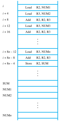
The Absolute mode can represent global variables in a program. A declaration such as Integer NUM1, NUM2, SUM; in a high-level language program will cause the compiler to allocate a memory location to each of the variables NUM1, NUM2, and SUM.
Whenever they are referenced later in the program, the compiler can generate assembly-language instructions that use the Absolute mode to access these variables. The Absolute mode is used in the instruction Load R2, NUM1
For example, the instruction Add R4, R6, 200immediate adds the value 200 to the contents of register R6, and places the result into register R4.
Warning
Using a subscript to denote the Immediate mode is not appropriate in assembly languages.
A common convention is to use the number sign (#) in front of the value to indicate that this value is to be used as an immediate operand. Hence, we write the instruction above in the form Add R4, R6, #200
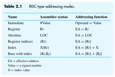
In the addressing modes that follow, the instruction does not give the operand or its address explicitly. Instead, it provides information from which an effective address (EA) can be derived by the processor when the instruction is executed. The effective address is then used to access the operand.
Branching
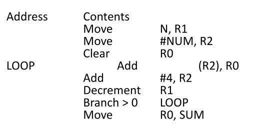
Consider the task of adding a list of n numbers. Separate Load and Add instructions are used to add each number to the contents of register R2. After all the numbers have been added, the result is placed in memory location SUM.
Instead of using a long list of Load and Add instructions, it is possible to implement a program loop in which the instructions read the next number in the list and add it to the current sum. To add all numbers, the loop has to be executed as many times as there are numbers in the list.
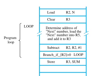
The body of the loop is a straight-line sequence of instructions executed repeatedly. It starts at location LOOP and ends at the instruction Branch_if_[R2]>0. During each pass through this loop, the address of the next list entry is determined, and that entry is loaded into R5 and added to R3. The address of an operand can be specified in various ways,
Assume that the number of entries in the list, n, is stored in memory location N, as shown. Register R2 is used as a counter to determine the number of times the loop is executed. Hence, the contents of location N are loaded into register R2 at the beginning of the program.
Then, within the body of the loop, Subtract R2, R2, #1 reduces the contents of R2 by 1 each time through the loop. Execution of the loop is repeated as long as the contents of R2 are greater than zero.
We now introduce branch instructions. This type of instruction loads a new address into the program counter. As a result, the processor fetches and executes the instruction at this new address, called the branch target, instead of the instruction at the location that follows the branch instruction in sequential address order.
A branch instruction causes a branch only if a specified condition is satisfied. If the condition is not satisfied, the PC is incremented in the normal way, and the next instruction in sequential address order is fetched and executed.
Branch_if_[R2]>0 LOOP
Condition Codes
The data conditions or status, after an arithmetic or logical operation are indicated by setting or clearing the flip – flops called flags or condition codes. Each flip-flop holding a data condition code is a one –bit storage cell (logic circuit) that can be set to a 1 or reset to 0 value.
These condition codes are set/reset as a result of arithmetic and logical operations in the ALU.
Results of various instructions are stored for subsequent use by conditional instructions. This is done by recording the required info in individual bits, called as condition code flags-grouped together in special processor register called as condition code register or status register.
Conditional Code Flags:
N – Negative
Z – Zero
V – Overflow
C – Carry
1 if results are Negative
0 if results are Positive
1 if results are Zero
0 if results are Non zero
1 if arithmetic overflow occurs
0 no overflow occurs
1 if carry from MSB bit
0 if there is no carry from MSB bit
Pentium processor makes use of following condition codes:
C (carry flag)
P (parity flag)
A (Auxiliary carry flag)
Z (zero flag)
S (sign flag)
O (over flow flag)
Addressing Modes
The compiler generates appropriate sequences of low-level instructions that implement the desired operations. The different ways for specifying the locations of instruction operands are known as addressing modes.
Example
Name Form Example Description Immediate $immmovl $-500,%raxRegister ramovl %rdx,%raxDirect Addressing immmovl 2000,%raxIndirect Adressing ramovl (%rdx),%rax
We access an operand by specifying the name of the register or the address of the memory location where the operand is located.
Immediate mode
Here the operand is specified in the instruction itself. An instruction that follows immediate mode has an operand field rather than an address field.
For example: Move 50immediate, R0
A common convention say, a pound symbol # has to precede the value of an
immediate operand Move #50, R0
Example
A=B+6 Move B,R1 Add #6,R1 Move R1,A
Absolute (Direct) mode
Here operand resides in Memory and its address is given explicitly in the address field of an instruction. This scheme need only one memory reference in addition to instruction fetch cycle and no further calculation is required to compute operand address.
Direct addressing scheme is simple to use and easy to implement without the requirement for additional hardware. However it offers only limited memory address space.
Example
Move LOC,R0 Load P Store S
Register mode
In this scheme, the operand is the contents of a register appearing in the
instruction i.e A=R
Example
Add R1, R2
Important
Advantages of this scheme :
- No memory reference
- A few bit address to indicate register location
- Speedy execution since register is inside the processor & has low access time.
Disadvantages of this scheme :
- Limited address space as number of registers are less in many of the processors.
Indirect mode
The effective address of the operand is the contents of a register or memory location whose address appears in the instruction By referring to this address (EA), the required operand can be fetched from memory.
Example
Add (A), R0 i.e. EA = (A) i.e. contents of A is B
Here B is effective address of desired operand in memory
Register Indirect
Here, instruction specifies a register in the CPU whose contents give the effective
address of the operand in Memory. For example Add (R1), R0 i.e. EA = (R1) i.e. contents of R1 is B
Tip
The advantage of Register Indirect Addressing:
- It uses one less memory reference (memory read operation)
- Address field of the instruction uses a fewer bits to specify a register
Register indirect addressing can be specified with Effective Address EA = (R) i.e. B
Advantages of Indirect addressing:
- a wider address range to refer to a large number of memory locations. Disadvantage of Indirect addressing:
- 2 or more memory references (memory read operations) required to fetch the desired operand in memory.
Indexed mode
Here, effective address of the operand is generated by adding a constant value to the contents of a register. This constant value may be either an offset value called
displacement or beginning address of data/operand array in main memory (Base).
Indexed addressing mode is symbolically represented as X(R)
Here X denote a constant and R is name of the register involved in Indexing.
Effective address EA of the operand is given as EA = X + [R]
Contents of index register are not changed during the process of address generation.
Example
A = 1040 = X; constant X corresponds to a memory location(R) = 20i.e. Index or offset value.EA = A + (R) = 1040 + 20 EA = 1060 at which you will find desired operand 50
You can use indexed addressing mode in two ways
-
A constant value X defines here beginning address of operand in memory and index register Ri contains offset value (Displacement). For example 1040 in the following instruction:
Add 1040 (R1), R2,X=1040 R1=20offset -
A constant value X defines an offset and index register Ri contains beginning address of operand in memory. For example 20 in the following instruction:
Add 20(R1), R2X=20 R1=1040 -
Index addressing is fast and is excellent for manipulating data structures such as arrays as all you need to do is set up a base address then use the index in your code to access individual elements.
-
Another advantage of indexed addressing is that if the array is re-located in memory at any point then only the base address needs to be changed. The code making use of the index can remain exactly the same.
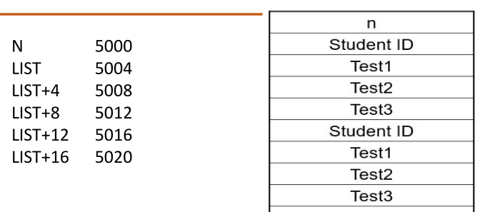
Several variations of this basic form provide a very efficient access to memory operands in practical programming situations. For example, a second register may be used to contain the offset X, in which case we can write the Index mode as (Ri, Rj).
The effective address is the sum of the contents of registers Ri and Rj.
- The second register is usually called the base register.
- This form of indexed addressing provides more flexibility in accessing operands, because both components of the effective address can be changed.
Another version of the Index mode uses two registers plus a constant, which can be denoted as X(Ri, Rj)
In this case, the effective address is the sum of the constant X and the contents of registers Ri and Rj. This added flexibility is useful in accessing multiple components inside each item in a record, where the beginning of an item is specified by the (Ri, Rj) part of the addressing mode.
Relative mode
This scheme supplies the relative position of the memory operand to be located. It’s like index mode only but program counter register PC substitutes for base address contents.
Example
Commonly used to specify the target address in branch instruction Relative Mode specify Effective Address by a notation:
X(PC)Effective address is
EA = [ PC ] + X
Branch > 0loop Here jump value / displacement± X
Auto increment mode
The EA of the operand is the contents of a register specified in the instruction. After accessing the operand, the contents of this register are incremented automatically to point to the next operand in contiguous memory locations.
Example
Notation for Auto Increment Mode: (Ri) +
For example: Add (R2) +, R0
Use of Auto Increment mode instruction eliminates the use of explicit increment instruction
Example
Program to add n numbers using autoincrement
	MOVE N,R1
	MOVE #NUM1,R2
	CLEAR R0
LOOP ADD (R2)+,R0
	DECREMENT R1
	BRANCH >0 LOOP
	MOVE R0,SUM
Auto decrement mode
Here, content of a register specified in the instruction is decremented to denote effective address of next operand in successive memory location.
Example
Notation for Auto Decrement Mode: - (Ri)
Add – (R2), R0It allows accessing of operands in decreasing order of memory address
Assembly
A complete set of such symbolic names and rules for their use constitutes a programming language, generally referred to as an assembly language.
ST R2, SUM
The mnemonic ST represents the binary pattern, or operation (OP) code, for the operation
performed by the instruction. The assembler translates this mnemonic into the binary OP
code that the computer recognizes.
Assembler
The assembler stores the object program on the secondary storage device available in the computer, usually a magnetic disk. The object program must be loaded into the main memory before it is executed. For this to happen, another utility program called a loader must already be in the memory. Executing the loader performs a sequence of input operations needed to transfer the machine-language program from the disk into a specified place in the memory.
The Assembly Process
After preparing the source file, it translates source programs written in an assembly language into object programs that comprise machine instructions. The assembler also converts the assembly-language representation of data into binary patterns that are part of the object program. After loading a source file from the disk into the memory and translating it into an object program, the assembler stores the object program in a separate file on the disk.
The source program uses mnemonics to represent OP codes in machine instructions. A
set of syntax rules governs the specification of addressing modes for the data operands of
these instructions. The assembler generates the binary encoding for the OP code and other
instruction fields.
The assembler recognizes directives that specify numbers and characters and directives that allocate memory space for data areas.
Using EQU (equate) directives, the programmer can define names that represent constants. These names can then appear in the source program as operands in instructions. Names can also be defined as address labels for branch targets, entry points of subroutines, or data locations in the memory.
Address labels are assigned values based on their position relative to the beginning of an assembled program. As the assembler scans through the source program, it keeps track of all names and their corresponding values in a symbol table. Each time a name appears, it is replaced with its value from the table.
Two-pass Assembler
A problem arises when a name appears as an operand before its value is defined. For example, this happens if a forward branch is required to an address label that appears later in the program.
A commonly-used solution to this problem is to have the assembler scan through the source program twice. During the first pass, it creates the symbol table. For EQU directives,
each name and its defined value are recorded in the symbol table. For address labels, the
assembler determines the value of each name from its position relative to the start of the
source program. The value is determined by summing the sizes of all machine instructions
processed before the definition of the name.
At the end of the first pass, all names appearing in the source program will have been assigned numerical values in the symbol table. The assembler then makes a second pass through the source program, looks up each name item counters in the symbol table, and substitutes the corresponding numerical value.
Loading Programs
Object programs generated by the assembler are stored in files on a disk. To execute a specific object program, it is first loaded from the disk into the memory. Then, the address of the first instruction to be executed is loaded into the program counter.
The loader transfers the object program from the disk into a specified place in the memory. It must know the length of the program and the address in the memory where it will be loaded. The assembler usually places this information in a header in the object file, preceding the machine instructions and data of the object program.
The loader starts its execution by branching to the first instruction to be executed. In the source program, the programmer indicates the first instruction with a special address label such as START. The assembler includes the value of this address label in the header of the object program.
Stacks
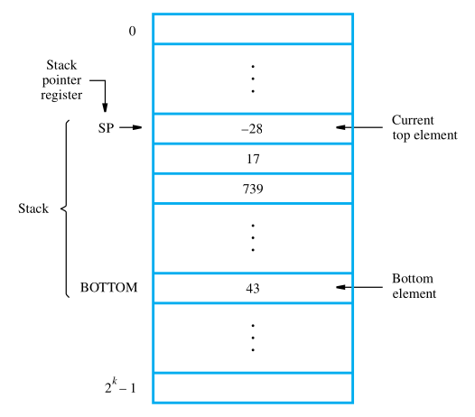
In modern computers, a stack is implemented by using a portion of the main memory for this purpose. One processor register, called the stack pointer (SP), is used to point to a particular stack structure called the processor stack.
Data can be stored in a stack with successive elements occupying successive memory locations. Assume that the first element is placed in location BOTTOM, and when new elements are pushed onto the stack, they are placed in successively lower address locations. We use a stack that grows in the direction of decreasing memory addresses, because this is a common practice.
The stack pointer, SP, is used to keep track of the address of the element of the stack that is at the top at any given time. If we assume a byte-addressable memory with a 32-bit word length, the push operation can be implemented as
Subtract SP, SP, #4
Store    Rj, (SP)
The Subtract instruction subtracts 4 from the contents of SP and places the result in
SP. Assuming that the new item to be pushed on the stack is in processor register Rj, the
Store instruction will place this value on the stack. These two instructions copy the word
from Rj onto the top of the stack, decrementing the stack pointer by 4 before the store (push) operation.
The pop operation can be implemented as
Load Rj, (SP)
Add   SP, SP, #4
These two instructions load (pop) the top value from the stack into register Rj and then
increment the stack pointer by 4 so that it points to the new top element.
Subroutines
For example, a subroutine may evaluate a mathematical function, or it may sort a list of values into increasing or decreasing order. It is possible to reproduce the block of instructions that constitute a subroutine at every place where it is needed in the program.
To save space, only one copy of this block is placed in the memory, and any program that requires the use of the subroutine simply branches to its starting location. When a program branches to this location it is known as “calling the subroutine”
Nesting
To have one subroutine call another. In this case, the return address of the second call is also stored in the link register, overwriting its previous contents. Hence, it is essential to save the contents of the link register in some other location before calling another subroutine. Otherwise, the return address of the first subroutine will be lost. Subroutine nesting can be carried out to any depth. Eventually, the last subroutine called completes its computations and returns to the subroutine that called it.
The return address needed for this first return is the last one generated in the nested call sequence. That is, return addresses are generated and used in a last-in–first-out order. This suggests that the return addresses associated with subroutine calls should be pushed onto the processor stack.
Correct sequencing of nested calls is achieved if a given subroutine SUB1 saves the return address currently in the link register on the stack, accessed through the stack pointer, SP, before it calls another subroutine SUB2. Then, prior to executing its own Return instruction, the subroutine SUB1 has to pop the saved return address from the stack and load it into the link register.
Using a High-level Language for I/O Tasks
Consider the following I/O task. A program uses the polling approach to read 8-bit characters from a keyboard and send them to a display as they are entered by a user.
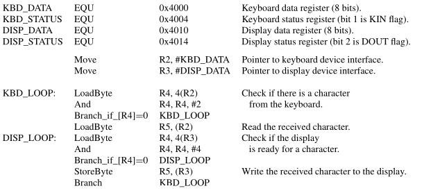
In C, a pointer may be set to any memory location, including a memory-mapped I/O location. The value of such a pointer is the address of the location in question. If the contents of this location are to be treated as a character, the pointer should be declared to be of character type. This defines the contents as being one byte in length, which is the size of the I/O registers.
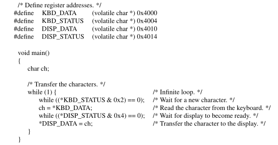
The define statements in are used to associate the required address constants with the symbolic names of the pointers. These statements serve the same purpose as the EQU statements. They enable the compiler to replace the symbolic names in the program with numeric values. The define statements also indicate the data type for the pointers. The compiler can then generate assembly-language instructions with known values and correct data sizes.
Standard I/O Interfaces
Because of electrical reasons only a few devices can be connected directly to the processor bus.
- Motherboard usually provides another bus that can support more devices.
- Processor bus and the other bus (called as expansion bus) are interconnected by a circuit called “bridge”.
- Devices connected to the expansion bus experience a small delay in data transfers.
- Design of a processor bus is closely tied to the architecture of the processor.
- No uniform standard can be defined.
- Expansion bus however can have uniform standard defined.
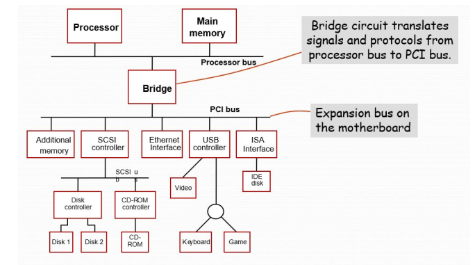
PCI BUS
- Peripheral Component Interconnect
- Introduced in 1992
- Low-cost bus
- Processor independent
- Plug-and-play capability
- In today’s computers, most memory transfers involve a burst of data rather than just one word. The PCI is designed primarily to support this mode of operation.
- The bus supports three independent address spaces: memory, I/O, and configuration.
- we assumed that the master maintains the address information on the bus until data transfer is completed. But, the address is needed only long enough for the slave to be selected. Thus, the address is needed on the bus for one clock cycle only, freeing the address lines to be used for sending data in subsequent clock cycles. The result is a significant cost reduction.
- A master is called an initiator in PCI terminology. The addressed device that responds to read and write commands is called a target.
Mount Actions
- PCI incorporates in each I/O device interface a small configuration ROM memory that stores information about that device.
- The configuration ROMs of all devices are accessible in the configuration address space. The PCI initialization software reads these ROMs and determines whether the device is a printer, a keyboard, an Ethernet interface, or a disk controller.
- It can further learn bout various device options and characteristics.
- Devices are assigned addresses during the initialization process. This means that during the bus configuration operation, devices cannot be accessed based on their address, as they have not yet been assigned one.
- Hence, the configuration address space uses a different mechanism. Each device has an input signal called Initialization Device Select,
IDSEL# - Electrical characteristics: PCI bus has been defined for operation with either a 5 or 3.3 V power supply.
SCSI Bus
Info
The acronym SCSI stands for Small Computer System Interface. It refers to a standard bus defined by the American National Standards Institute (ANSI) under the designation X3.131. In the original specifications of the standard, devices such as disks are connected to a computer via a 50-wire cable, which can be up to 25 meters in length and can transfer data at rates up to 5 megabytes/s. The SCSI bus standard has undergone many revisions, and its data transfer capability has increased very rapidly, almost doubling every two years. SCSI-2 and SCSI-3 have been defined, and each has several options. Because of various options SCSI connector may have 50, 68 or 80 pins.
-
Devices connected to the SCSI bus are not part of the address space of the processor
-
The SCSI bus is connected to the processor bus through a SCSI controller.
-
This controller uses DMA to transfer data packets from the main memory to the device, or vice versa.
-
A packet may contain a block of data, commands from the processor to the device, or status information about the device. A controller connected to a SCSI bus is one of two types – an initiator or a target.
-
An initiator has the ability to select a particular target and to send commands specifying the operations to be performed. The disk controller operates as a target. It carries out the commands it receives from the initiator.
-
The initiator establishes a logical connection with the intended target. Once this connection has been established, it can be suspended and restored as needed to transfer commands and bursts of data. While a particular connection is suspended, other device can use the bus to transfer information. This ability to overlap data transfer requests is one of the key features of the SCSI bus that leads to its high performance.
-
Data transfers on the SCSI bus are always controlled by the target controller.
-
To send a command to a target, an initiator requests control of the bus and, after winning arbitration, selects the controller it wants to communicate with and hands control of the bus over to it.
-
Then the controller starts a data transfer operation to receive acommand from the initiator.
-
Data transfers on the SCSI bus are always controlled by the target controller.
-
To send a command to a target, an initiator requests control of the bus and, after winning arbitration, selects the controller it wants to communicate with and hands control of the bus over to it.
-
Then the controller starts a data transfer operation to receive a command from the initiator.
Read Over SCSI
Example
Assume that processor needs to read block of data from a disk drive and that data are stored in disk sectors that are not contiguous. The processor sends a command to the SCSI controller, which causes the following sequence of events to take place:
- The SCSI controller, acting as an initiator, contends for control of the bus.
- When the initiator wins the arbitration process, it selects the target controller and hands over control of the bus to it.
- The target starts an output operation (from initiator to target); in response to this, the initiator sends a command specifying the required read operation.
- The target, realizing that it first needs to perform a disk seek operation, sends a message to the initiator indicating that it will temporarily suspend the connection between them. Then it releases the bus.
- The target controller sends a command to the disk drive to move the read head to the first sector involved in the requested read operation. Then, it reads the data stored in that sector and stores them in a data buffer. When it is ready to begin transferring data to the initiator, the target requests control of the bus. After it wins arbitration, it reselects the initiator controller, thus restoring the suspended connection.
- The target transfers the contents of the data buffer to the initiator and then suspends the connection again
- The target controller sends a command to the disk drive to perform another seek operation. Then, it transfers the contents of the second disk sector to the initiator as before. At the end of this transfers, the logical connection between the two controllers is terminated.
- As the initiator controller receives the data, it stores them into the main memory using the DMA approach.
- The SCSI controller sends as interrupt to the processor to inform it that the requested operation has been completed
USB
Universal Serial Bus (USB) is an industry standard developed through a collaborative effort of several computer and communication companies, including Compaq, Hewlett-Packard, Intel, Lucent, Microsoft, Nortel Networks, and Philips.
To accommodate a large number of devices that can be added or removed at any time, the USB has the tree structure as shown in the figure.
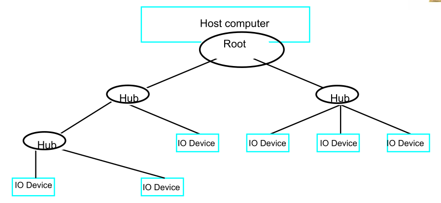
- Each node of the tree has a device called a hub, which acts as an intermediate control point between the host and the I/O devices. At the root of the tree, a root hub connects the entire tree to the host computer. The leaves of the tree are the I/O devices being served (for example, keyboard, Internet connection, speaker, or digital TV)
- In normal operation, a hub copies a message that it receives from its upstream connection to all its downstream ports. As a result, a message sent by the host computer is broadcast to all I/O devices, but only the addressed device will respond to that message. However, a message from an I/O device is sent only upstream towards the root of the tree and is not seen by other devices. Hence, the USB enables the host to communicate with the I/O devices, but it does not enable these devices to communicate with each other.
- To accommodate a large number of devices that can be added or removed at any time, the USB has the tree structure as shown in the figure.
- Each node of the tree has a device called a hub, which acts as an intermediate control point between the host and the I/O devices. At the root of the tree, a root hub connects the entire tree to the host computer. The leaves of the tree are the I/O devices being served (for example, keyboard, Internet connection, speaker, or digital TV)
- In normal operation, a hub copies a message that it receives from its upstream connection to all its downstream ports. As a result, a message sent by the host computer is broadcast to all I/O devices, but only the addressed device will respond to that message.
- However, a message from an I/O device is sent only upstream towards the root of the tree and is not seen by other devices. Hence, the USB enables the host to communicate with the I/O devices, but it does not enable these devices to communicate with each other.
USB Addessing
Info
When a USB is connected to a host computer, its root hub is attached to the processor bus, where it appears as a single device. The host software communicates with individual devices attached to the USB by sending packets of information, which the root hub forwards to the appropriate device in the USB tree.
Each device on the USB, whether it is a hub or an I/O device, is assigned a 7-bit address. This address is local to the USB tree and is not related in any way to the addresses used on the processor bus.
A hub may have any number of devices or other hubs connected to it, and addresses are assigned arbitrarily. When a device is first connected to a hub, or when it is powered on, it has the address 0. The hardware of the hub to which this device is connected is capable of detecting that the device has been connected, and it records this fact as part of its own status information. Periodically, the host polls each hub to collect status information and learn about new devices that may have been added or disconnected.
When the host is informed that a new device has been connected, it uses a sequence of commands to send a reset signal on the corresponding hub port, read information from the device about its capabilities, send configuration information to the device, and assign the device a unique USB address. Once this sequence is completed the device begins normal operation and responds only to the new address.
USB protocols
All information transferred over the USB is organized in packets, where a packet consists of one or more bytes of information. There are many types of packets that perform a variety of control functions. The information transferred on the USB can be divided into two broad categories: control and data. Control packets perform such tasks as addressing a device to initiate data transfer, acknowledging that data have been received correctly, or indicating an error.
Data packets carry information that is delivered to a device. A packet consists of one or more fields containing different kinds of information. The first field of any packet is called the packet identifier, PID, which identifies the type of that packet.
They are transmitted twice. The first time they are sent with their true values, and the second time with each bit complemented The four PID bits identify one of 16 different packet types. Some control packets, such as ACK (Acknowledge), consist only of the PID byte.
Inochronous Traffic on USB
One of the key objectives of the USB is to support the transfer of isochronous data. Devices that generates or receives isochronous data require a time reference to control the sampling process. To provide this reference. Transmission over the USB is divided into frames of equal length.
A frame is 1ms long for low-and full-speed data. The root hub generates a Start of Frame control packet (SOF) precisely once every 1 ms to mark the beginning of a new frame.
The arrival of an SOF packet at any device constitutes a regular clock signal that the device can use for its own purposes. To assist devices that may need longer periods of time, the SOF packet carries an 11-bit frame number.
Following each SOF packet, the host carries out input and output transfers for isochronous devices. This means that each device will have an opportunity for an input or output transfer once every 1 ms.
Electrical Characterestics of USB
- The cables used for USB connections consist of four wires.
- Two are used to carry power, +5V and Ground.
- The other two wires are used to carry data. Different signaling schemes are used for different speeds of transmission.
- At low speed, 1s and 0s are transmitted by sending a high voltage state (5V) on one or the other o the two signal wires. For high-speed links, differential transmission is used.
Info
Thus, a hub or an I/O device may be powered directly from the bus, or it may have its own external power connection.
Accessing I/O devices
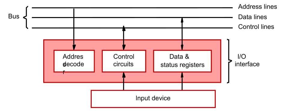
Memory mapped I/O
Some memory addresses refer to peripheral device buffer registers, such as
DATAIN,DATAOUT. Data can be transferred b/w the cpu and these registers using same set of instructions and same status flags
Example
- Ex: MoveByte DATAIN,R0
- MoveByte R0,DATAOUT
- Status flags SIN and SOUT can be included device status register
- Assume that the bit b3 of the status registers
INSTATUS,OUTSTATUScorresponds toSINandSOUT
Connected to the bus using an I/O interface circuit
- Address decoder, control circuit, and data and status registers.
- Address decoder decodes the address placed on the address lines thus enabling the device to recognize its address.
- Data register holds the data being transferred to or from the processor.
- Status register holds information necessary for the operation of the I/O device.
- Data and status registers are connected to the data lines, and have unique addresses.
- The Address decoder, the data & status register and the control circuitry required to coordinate I/O transfer constitute the Device’s interface circuit.
Program-controlled I/O
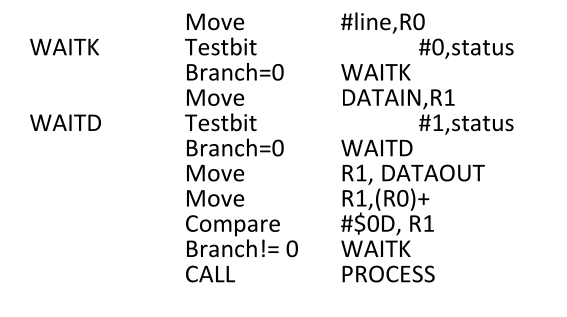
- Processor repeatedly monitors a status flag to achieve the necessary synchronization.
- Processor polls the I/O device.
- Two other mechanisms used for synchronizing data transfers between the processor and memory:
- Interrupts.
- Direct Memory Access.
- A status flag i.e.
SINandSOUTis included in the interface circuit as part of the status register. - This flag is set to 1 when a char is entered at the keyboard and and set to 0 when the char is read by the processor .
- Same for
SOUT
Mechanism of I/O transfer between processor and keyboard & video monitor:
-
A character key when pressed from the keyboard its scan code is sent to an 8-bit buffer register DATAIN in the keyboard.
-
Processor is informed about a valid character data presence in DATAIN register by setting a synchronization flag SIN to 1.
-
I/O driver program continuously monitors contents of SIN flag, & when SIN is set to 1, it reads the contents of DATAIN.
-
Thus character stored in DATAIN register is transferred to processor over a system bus and SIN content is automatically reset to 0.
-
A similar set of events take place while transferring a character data from processor to the display screen.
-
Here a DATAOUT register that holds a character’s code to be displayed when synchronization control flag SOUT is set to 1. When SOUT equals 1, the display device is ready to receive a character from processor.
-
The transfer of a character to DATAOUT resets SOUT to 0.
-
I/O driver program instructions control the status of SOUT flag.
The buffer registers DATAIN, DATAOUT, and control flags SIN, SOUT in this hardware setup forms parts of a connectivity circuits commonly known as device interface or interface hardware.
- I/O driver program instructions for I/O data transfer
- SOUT is set to 1 when display terminal is free to display next character.
- The wait loop is executed repeatedly until the control flag SOUT is set to 1 by the display terminal.
- Initial state of SIN is 0 and SOUT is 1
Ex: Keyboard and a display device.
- The 4 regs involved in the data transfer operations are: DATAIN, DATAOUT, STATUS, CONTROL
- STATUS reg contains two control flags SIN and SOUT and two flags KIRQ, DIRQ which are used in conjunction with interrupts.
Handling Multiple Devices
When a request is received over the common interrupt-request line, additional information is needed to identify the particular device that activated the line.
- The additional information is available in its status register. KIRQ & DIRQ.
- Then ISR polls all the I/O devices connected to the bus.
- The first device with its IRQ bit set is the device that should be serviced.
An appropriate subroutine is called to provide the request service.
- The polling scheme is easy to implement , but it spends time in interrogating the IRQ bits of all the devices that may not be requesting any service.
- An alternative approach is to use vectored interrupts.